Map temperatures to a PCB structural model
Practice aligning source and target models for mapping the temperature results from thermal model to the structural model and use these temperature results as a temperature load for the structural model.
Open and explore the thermal Simulation file
Open the Simulation file and reset the dialog box settings.
- Choose File→Open and open pcb_mapping/pcb_thermal_sim.sim.
- Choose File→Preferences→User Interface and on the Dialog and Precision page, reset the dialog box memory.
-
Expand and explore all nodes in the Simulation
Navigator.
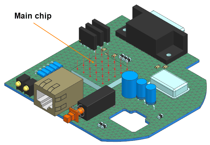
A printed circuit board (PCB) has many components. This thermal model focuses on the main chip (CPU). Notice that triangular type elements are used to mesh the PCB. The following boundary conditions are defined in the solved thermal model:- Thermal coupling between the CPU and PCB.
- Radiation thermal coupling between the CPU and PCB.
- Forced convection to environment on PCB and on the CPU.
- 10 W heat load on the CPU.
Display the thermal results
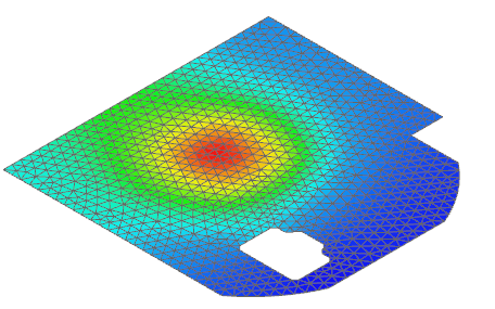
Load and display the temperatures on the PCB thermal model, which is the source model. You will map these temperature results onto the structural model, which is the target model later.
- In the Post Processing Navigator, double-click the Thermal-Flow node, expand it and double-click the Temperature - Elemental node.
-
Expand the Post View 1→pcb_thermal_fem.fem→2D Elements nodes and hide CPU Collector to display temperature on the PCB.
-
Choose Results tab→Context
group→Return to Home
 .
.
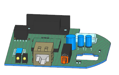
Open the structural solution
Open the file that contains Simcenter Nastran structural FEM and Simulation files.
Create the mapping solution
Create the mapping solution in the structural Simulation file that points to the thermal solution results.
-
Choose Home tab→Solution
group→Solution
 .
.
-
In the Solution group, from the Solver list, select one of the following options: Simcenter 3D Thermal/Flow, Simcenter 3D Electronic Systems Cooling, Simcenter 3D Space Systems Thermal.
Note that for this activity the Simcenter 3D Thermal/Flow solver is selected.
- From the Analysis Type list, select Mapping.
- Click Create Solution.
-
On the Mapping Details tab, in the Data Source and Destination group, click Browse
 and select the pcb_thermal_sim-CPU_10W_loadcase.bun file.
- Click OK.
- On the Optional Output tab, in the Output Format group, select the Create Nastran Solution check box.
- Click OK.
Align source and target models
Align the source and target models, before solving the mapping solution.
-
Choose Home tab→Loads and
Conditions group→Simulation Object
Type→Source Model Mapping
 .
.
- In the Source Model group, click Browse and select the pcb_thermal_sim-CPU_10W_loadcase.xml file that contains thermal model mesh data.
-
In the Alignment group, click Align
Source Model
 .
.
In the graphics window, the source model is displayed as a blue wireframe. - In the Preview group, select the Preview check box.
-
In the graphics window, select the source (1) and target (2) nodes.
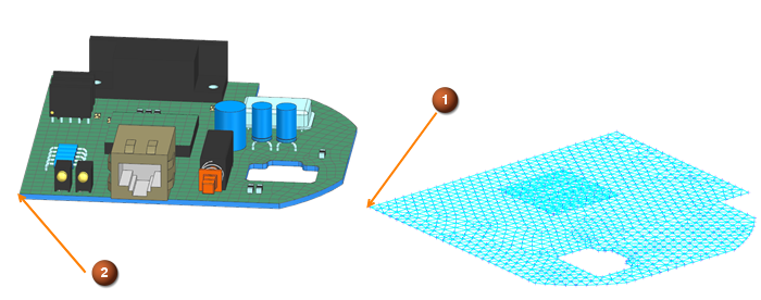
- Click Add Pair.
-
Repeat the steps 5 and 6 for the following source and target node
pair.
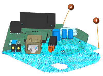
- Click Align.
- Click OK all dialog boxes.
Solve the mapping solution
Solve the mapping solution you just created on the structural model.
- In the Simulation Navigator, right-click the Solution 1 node and choose Solve.
- In the Solve dialog box, click OK.
- Wait for the mapping solve to end, before proceeding.
- In the Analysis Job Monitor dialog box, click Cancel.
- Close the Information window.
Display mapped thermal results
Display the mapped temperatures on the structural PCB model.
- In the Simulation Navigator, under the Solution 1 node, double-click the Results node.
- In the Post Processing Navigator, expand the Thermal-Flow node and double-click the Temperature – Nodal node.
-
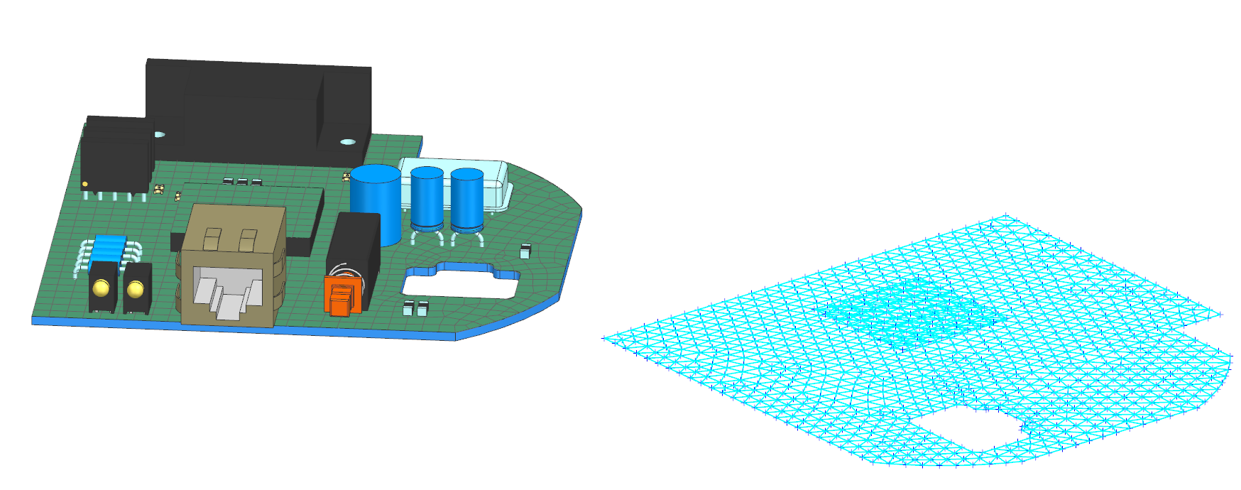
Expand the Post View 2→pcb_structural_fem.fem→2D Elements nodes and hide CPU Collector to display temperature on the PCB.
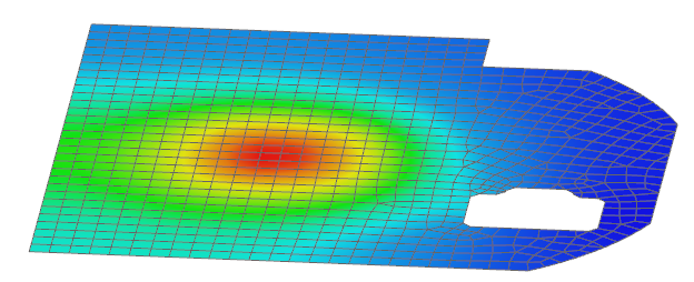
The temperatures were mapped from triangular thermal elements to quad structural elements. -
Choose Results tab→Context
group→Return to Home
.
Constrain the PCB and chip
Apply a fixed constraint at all corners of the PCB to constrain the model before solving.
- In the Simulation Navigator, double-click the Mapping Nastran node to activate the solution.
- Expand the Subcase1→Loads→Temperature Set – Temperature1 nodes to observe the temperature load, which was created by the mapping process.
- Expand the pcb_structural_fem.fem node and hide the polygon geometry and temperature symbols.
-
Choose Home tab→Loads and
Conditions group→Constraint Type
list→Fixed Constraint
 .
.
- On the Top Border bar, from the Type Filter list, select Node.
-
Select the following eight nodes on the model.
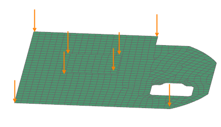
- Click OK.
- Click OK on the message dialog box.
Solve the structural solution
Solve the structural model with the temperature preload.
- In the Simulation Navigator, right-click the Mapping Nastran node and choose Solve.
- Click OK.
- Wait for the solve to end, before proceeding.
- In the Review Results dialog box, click No.
- In the Analysis Job Monitor dialog box, click Cancel.
- Close the Information window.
Display the structural results
Display displacement results on the PCB.
- In the Simulation Navigator, double-click the Results node.
-
In the Post Processing Navigator, expand the
Structural node, and double-click the
Displacement Nodal node.
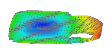
The average displacement is approximately 0.05 mm shows the deformation of PCB cause by the temperature gradient through the board.