Run a thermal analysis of an imported ECAD assembly
Practice setting up and solve an imported ECAD printed circuit board (PCB) assembly using PCB Exchange.
Open the part file
Open the part file and reset the dialog box settings.
- Choose File→Open and open pcbxesc\board_thermal.prt.
-
Choose
File→Preferences→User
Interface and on the Dialog and
Precision page, reset the dialog box memory.
Set PCB Exchange preferences
Set the read/write directory for your model, modify the board and component thermal settings, and set the default component dissipation to 0.
-
Choose Home tab→Data Exchange
group→Preferences
 .
.
-
On the General tab, next to the Read/Write Directory box, click Browse
 and navigate to the pcbxesc folder.
The software writes the log and temporary files in this directory.
and navigate to the pcbxesc folder.
The software writes the log and temporary files in this directory. - On the Board tab, in the Thermal Analysis group, select the Element Color swatch, and then select the color you want in the color palette.
- On the Components tab, in the Thermal Model group, in the Model list, make sure that Dissipation Only is selected.
- In the Dissipation box, type 0 W.
- In the Mesh Settings group, from the Element Size list, select Specify.
- In the Element Size box, type 3 mm.
- From the Element Thickness list, select Specify.
- In the Element Thickness box, verify that the value is set to 3 mm.
- Click OK.
Calculate the board conductivity
Compute the board conductivity from the board entities, such as vias, pads, and traces, stored in an independent entity file for this model.
-
Choose Home tab→Simulation
group→Board Properties
 .
.
- In the Calculations group, from the Thermal Algorithm list, select Discretized to calculate the thermal conductivities of each calculation point in the X and Y directions and create a thermal conductivity spatial field that is used in a 2D mesh collector.
- In the Settings group, from the Board Stackup list, select From File.
- Next to the Board Stackup File box, click Browse and select the pcbxesc\board_traces_info.cad file.
- Set the Number of Calculation Points to 200.
- In the Output group, in the Board Property File box, type board_thermal.xml.
- Select the View Calculation Report check box to generate an HTML report containing the images of the layers used to calculate the thermal conductivity of the board.
- Click OK.
- Close the Information window.
-
In the Web Browser
 tab, explore the
Board's Thermal Conductivity Calculation
Information report.
tab, explore the
Board's Thermal Conductivity Calculation
Information report.
-
Notice the thermal conductivity in X direction for the first layer of the
board.
Create the thermal solution
create a thermal solution using the computed board thermal conductivity and the component simulation database provided for this activity in the component.xml file. You will first generate the thermal database report to inspect from where the components will get their mesh and thermal settings.
- Choose File→Open and open pcbxesc\board_thermal.prt.
- Choose File→Preferences→User Interface and on the Dialog and Precision page, reset the dialog box memory.
- Choose Home tab→Data Exchange group→Validate Drop-down list→Thermal Database Report.
-
In the Web Browser tab, explore the
Thermal Database Report.
Notice that the component with D203 in the Reference Designator column will get its mesh and thermal settings from the STTH60L04W item in the component simulation database.
- Close the Information window.
- Open the component.xml file in a text editor and observe the content.
- Find the STTH60L04W item and notice that dissipation load is set to 2.0.
- Close the file without saving.
- Choose Home tab→Simulation group→Thermal Solution .
- In the Output Options group, select Use Component Simulation Database check box.
- Next to the Use Component Simulation Database box,click Browse and select the component.xml file.
- In the Output Options group, select the Board Thermal Conductivity from File check box.
- Next to the Board Thermal Conductivity from File box, click Browse and select the board_thermal.xml file.
-
Click OK to close both dialog boxes.
The software enters the Pre/Post application and creates the FEM and Simulation files.
-
Close the Information window.
Review the created Simulation file
Review the created solution.
-
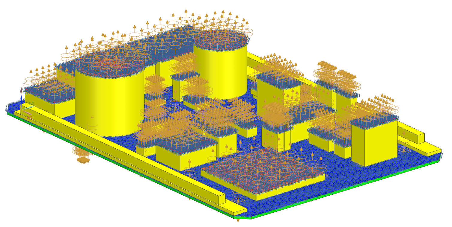
In the Simulation Navigator, expand the Simulation Object Container and Constraint Container nodes.
The solution contains the following boundary conditions:
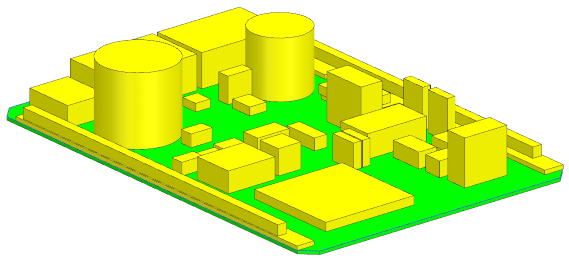
- The Printed Circuit Board simulation object, called Board, is defined for the board.
- The PCB Component simulation objects, which define the thermal model of the components, are organized by reference designator. There are 44 PCB Component simulation objects created.
- A Convection to Environment constraint, called Environment Convection, is defined on the board and all its components.
- In the Simulation Navigator, expand the Solution1→Constraint Set nodes.
- Under the Constraint Container node, right-click the Environment Convection node and choose Information.
- Examine the constraint information and close the Information window.
- Expand the Simulation Objects node and explore the simulation objects.
-
Hide the Simulation Objects and Constraint Set nodes to hide the boundary conditions.
Notice that the board mesh color is the one you chose.
Review the created FEM
Inspect the Board mesh collector, which has the information about board layers and their orthotropic thermal conductivity computed by PCB Exchange.
- In the Simulation Navigator, right-click the board_thermal_f.fem node and choose Make Work Part.
- Expand the board_thermal_f.fem→2D Collectors nodes.
-
Right-click the Board node and choose Edit.
The Board mesh collector references the PCB Stack physical property. Examine the Default mesh collector settings.
-
In the Physical Property group, in the PCB Stack Property row, click Edit.
The PCB Stack physical property contains PCB Layer and PCB Via modeling objects.
- On the Stack Definition tab, from the stack layer table, select Ply_1Conductive_1 and click Edit.
-
Observe the settings in the Ply_1_Conductive_1 PCB layer modeling object.
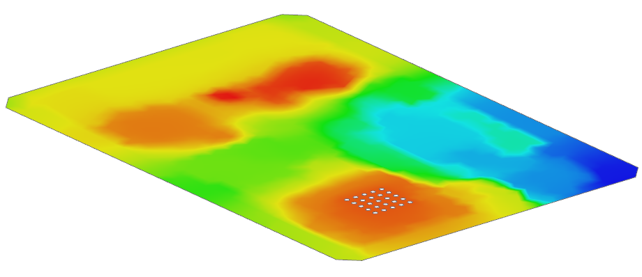
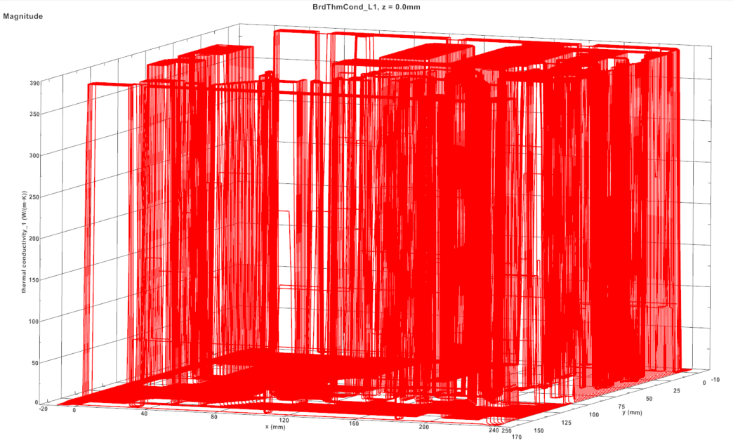
Notice that the thermal conductivity references the BrdThmCod_L1 field, which you will plot later.
- Click Cancel.
- On the Vias Definition tab, from the vias table, select the Via_31 and click Edit.
- Observe the settings in the Via_31 PCB via modeling object.
- Click Cancel to close all dialog boxes.
Review the board layer fields
-
In the Simulation Navigator, under the board_thermal_f.fem node, expand the Fields node.
A field is created for each board layer.
-
Right-click the BrdThmCond_L1 node and choose
Plot (XYZ)
 .
.
- Click OK.
-
In the Viewport dialog box, click Create
a New Window to Plot
 .
.
- Close Graph Window 1.
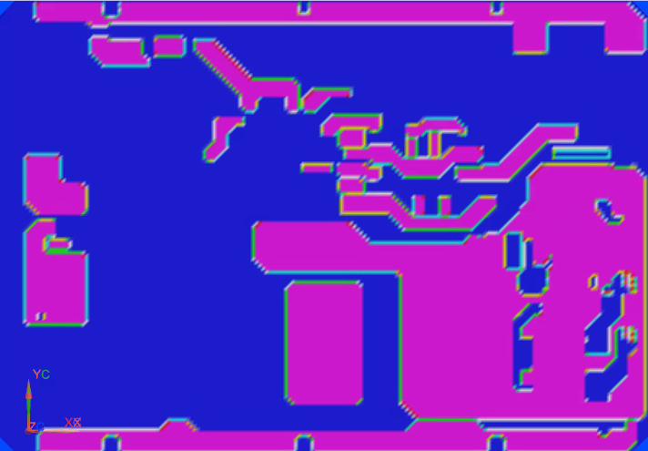
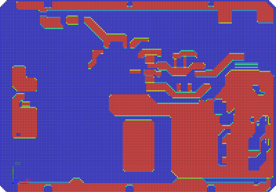
- In the Simulation Navigator, hide the Polygon Geometry and 2D Collectors nodes and show the BrdThmCod_L1 field.
- Right-click the BrdThmCod_L1 node, and select Edit Display.
- On the Results tab, in the Calculated Values group, from the Display Type list, select Contours.
- Click Apply.
- In the Source Table Values group, from the Display Type list, select Contours.
- Move Offset to Large.
-
Click OK.
Modify the dissipation loads
Modify the dissipation loads for components directly changing the values in the Expressions dialog box instead of modifying each of the seven PCB Component simulation objects separately.
- In the Simulation Navigator, right-click the board_thermal_s.sim and choose Make Work Part.
-
Under the Simulation Objects node, right-click the D203 node and choose Information.
Notice that the dissipation is set to 2W. The part number is STTH60L04W, which is an item defined in the component.xml file explored earlier.
- Close the Information window.
-
Right-click the D301 node and choose Information.
Notice that the dissipation is set to 0, which comes from the default value you specified in the PCB Exchange Preferences dialog box.
- Close the Information window.
-
Choose Tools tab→Utilities
group→Expressions
 .
.
- In the table, in the Name column, find the D203 expression, and in the Formula column, change its value to 0.2.
-
Do the same for the following heat loads:
- D205 = 0.15
- D207 = 0.15
- L301 = 2
- L401 = 2
- Q516 = 0.5
- T402 = 3
- Click OK.
-
In the Simulation Navigator, right-click the D203 node and choose Information.
Notice that the dissipation changed to 0.2 W.
- Close the Information window.
Solve the model
Solve the model.
-
Choose Home tab→Solution
group→Solve
 .
.
- Click OK.
- In the Review Results dialog box, click No.
- Wait for the solve to end, before proceeding.
- Close the Information window.
- In the Analysis Job Monitor dialog box, click Cancel.
Import the UNV file
Load generated UNV file to observe the resultant kx conductivities.
- In the Post Processing Navigator, right-click the Imported Results node and select Import Results.
- Click Browse, and select board_thermal.unv.
- Click OK.
-
In the Post Processing Navigator, expand board_thermal→Current Density Area - Elemental→X.
Display temperatures
Display the temperature results for the whole model and for only the board.
- In the Post Processing Navigator, under the Solution 1 node, double-click the Thermal-Flow node.
- In the Post Processing Navigator, expand the Thermal-Flow node and double-click the Temperature - Nodal node.
-
Choose Results tab→Display
group→Edge Style
drop-down→Feature
 .
.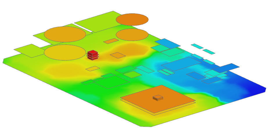
- In the Post Processing Navigator, expand the Post View 1→Mesh Collectors→board_thermal_f.fem→2D Elements nodes.
-
Hide 0D Elements and both 2D
Elements nodes and select the Board
to show the temperature distribution on the board.