Perform a heat transfer analysis between a chip, PCB, and casing
You will practice using different thermal-coupling types, and understand the options in the Thermal Coupling dialog box. You will also understand the role of primary and secondary regions selection in thermal couplings.
Open the Simulation file
Open the model Simulation file and reset the dialog box settings.
- Choose File→Open and open chip_pcb_case\chip_pcb_case_sim1.sim.
- Choose File→Preferences→User Interface, on the Dialog and Precision page, click Reset Dialog Memory.
- Click OK.
Explore the model
Explore the assembly FEM and mesh collectors.
-
In the Simulation Navigator, expand the chip_pcb_case_fem.fem node and click
 to hide the 2D Collectors node.
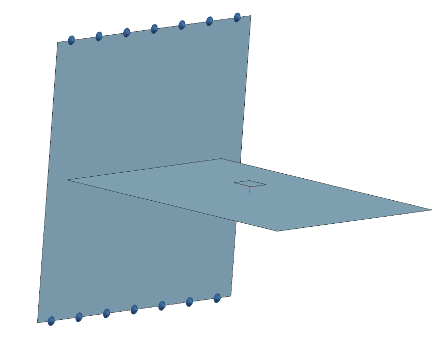
The model contains an underlying geometry, which is meshed using 2D elements. You can use these surfaces to apply boundary conditions. However, in this activity, you will learn how to apply simulation objects using elements. -
Click
 to show the 2D Collectors node.
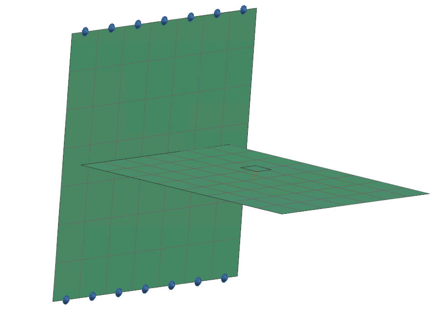
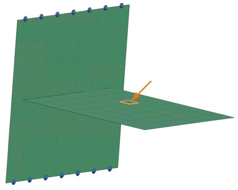
Define thermal couplings: chip to PCB
Define heat transfer coefficient thermal coupling between the chip and PCB.
For the first thermal coupling analysis, we will assume:
- The solder material between the chip and pcb has a thermal conductivity of k=100 W/m·K.
- The area ratio, Aratio, between the solder and the chip is 0.5.
- The gap between the chip and the PCB, Lgap, is 10 mm.
We can then define a heat transfer coefficient thermal coupling of h=k·Aratio/Lgap= 5000 W/(m2·°C).
-
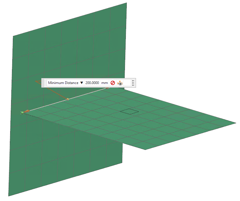
Choose Home tab→Loads and
Conditions group→Simulation Object
Type→Thermal Coupling
 .
.
- From the Type list, ensure Thermal Coupling is selected
- In the Name box, type Chip to Board.
- In the Primary Region group, from the Filter Type list, select 2D Elements.
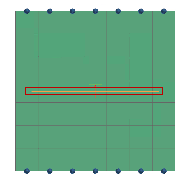
-
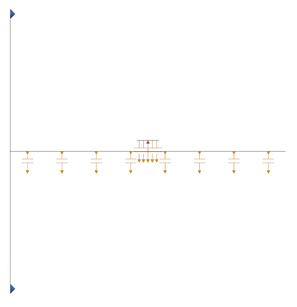
Select the elements in the graphics window as shown.
-
In the Secondary Region group, click
Select Object
 .
.
- From the Top Border Bar, from the Type Filter list, select Element.
- In the Secondary Region group, from the Filter Type list, select 2D Elements.
-
Select the 56 elements shown in the graphics window.
Tip: Press F8 for an orthogonal view. - In the Magnitude group, from the Type list, select Heat Transfer Coefficient .
- In the Coefficient box, type 5000 W/(m2·°C.
-
In the Additional Parameters group, clear the Only Connect Overlapping Elements check box.
The solver connects each primary sub-element to the closest secondary element.
- Click OK.
Define thermal couplings: PCB to case
Define heat transfer coefficient thermal coupling between the PCB edge and casing.
-
Rotate the model to view from the side.
-
In the Simulation Navigator, expand
Solution 1 node, right-click
Simulation Objects and select New
Simulation Object→ Thermal Coupling
.
- In the Name box, type PCB Edge to Casing.
- From the Top Border Bar, from the Type Filter list, select Element Edge.
- In the Primary Region group, from the Filter Type list, select 1D Elements.
-
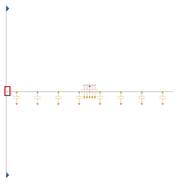
Select the 7 objects shown in the graphics window.
-
In the Secondary Region group, click
Select Object
.
- From the Top Border Bar, from the Type Filter list, select Element.
- From the Filter Type list, select 2D Elements.
-
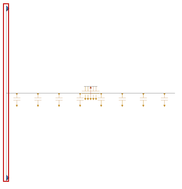
Select the 49 side elements shown in the graphics window.
- In the Magnitude group, select Heat Transfer Coefficient from the Type list.
- In the Coefficient box, type 1600 W/(m2·°C).
- Click OK.
Solve the model
Solve the thermal model and monitor its completion status.
- Right-click Solution 1 in Simulation Navigator and choose Solve.
- Click OK.
- Wait for Completed status in Analysis Job Monitor.
- In the Review Results dialog, click No.
- Close the Information window.
- Click Cancel in the Analysis Job Monitor dialog.
Post process results 1/4
Visualize nodal temperature results and thermal conductance between components.
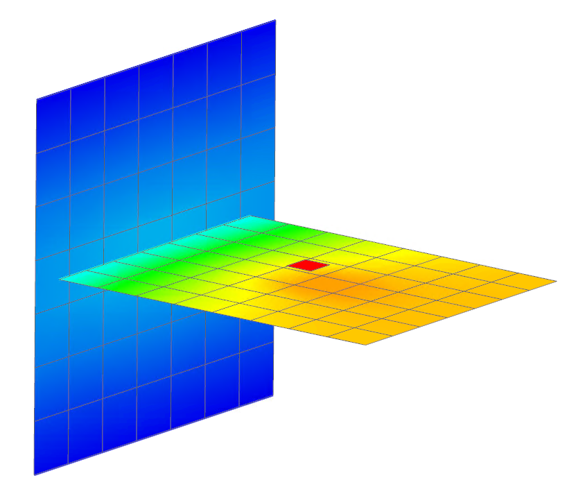
- In the Simulation Navigator, double-click Results node.
-
In the Post Processing Navigator, expand the
Thermal-Flow node, and double-click
Temperature – Nodal node.
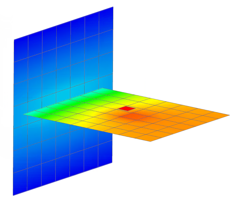
Results show that the heat flows from the chip to the PCB board because the PCB temperature increased in the vicinity of the chip. The software created a thermal conductance from the chip to the closest element on the PCB.
The temperature gradients on the board and the casing show that the board is also thermally connected to the casing. The software created conductances from the elements on the board edge to the overlapping 2D elements on the casing.
Using length proportional coefficients in thermal couplings
Calculate and apply equivalent conductances using length proportional coefficients.
The length of the contact edge is 0.2 m, and the original conductance between the PCB and the casing was defined as h=1600 W/(m2·°C). With these values we can calculate equivalent conductances. For example:
- An equivalent Total Conductance is Board-Casing Conductance = h × board_length × board_thicknessBoard-Casing Conductance = 1600 W/(m2·°C) × 0.2 m × 0.0015 m = 0.48 W/°C
- An equivalent Conductance per Length coefficient is Board–Casing
Conductance per Length = 0.48W/°C / 0.2m = 2.4 W/m·°C
-
Choose Results tab→Context group→Return to Home
 .
.
- In the Simulation Navigator, expand Simulation Object Container, right-click PCB Edge to Casing node and select Edit.
- In the Magnitude group, from the Type list, select Edge Contact.
- In the Conductance per Length box, specify 2.4 W/(m·°C).
- Click OK.
- Solve the model as described earlier.
Post process results 2/4
Visualize results with different thermal coupling types and boundary conditions.
- In the Simulation Navigator, double-click Results node.
-
In the Post Processing Navigator, expand the
Thermal-Flow node and double-click
Temperature – Nodal node.
- Observe results are consistent with prior analysis.
Analyze the effect of the heat transfer coefficient
Modify the heat transfer coefficient to observe its effect on temperature.
-
Choose Results tab → Context group → Return to Home
.
- In the Simulation Navigator, right-click Chip to Board node and select Edit.
- Set Coefficient to 1000 W/(m2·°C).
- Click OK.
- Solve the model.
Post process results 3/4
Visualize temperature changes due to coefficient modification.
- In the Simulation Navigator, double-click Results node.
-
In the Post Processing Navigator, expand the
Thermal-Flow node and double-click
Temperature – Nodal node.
Temperatures have increased a couple of degrees. The heat is not flowing out of the chip into the PCB as efficiently as before.
Analyze the effect of inverting primary and secondary surfaces
Swap primary and secondary surfaces and analyze the thermal impact.
-
Choose Results tab → Context group → Return to Home
.
- In the Simulation Navigator, right-click Chip to Board and select Edit.
-
Click Swap Regions
 to reverse primary and secondary regions.
- In the Additional Parameters group, make sure that the Only Connect Overlapping Elements check box is cleared.
- Click OK.
- Solve the model.
Post process results 4/4
Visualize the impact of inverting surfaces and verify correct coupling.
- In the Simulation Navigator, under Solution 1, double-click Results node.
-
In the Post Processing Navigator, expand
Thermal-Flow and double-click
Temperature – Nodal.
Note that the smaller surface should contain the primary elements when modeling conduction between surfaces in contact. Heat flow between the primary and secondary elements will then be limited to adjacent elements.
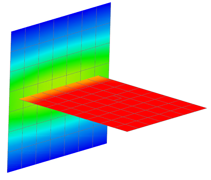
Notice that the results are incorrect. The solver created a thermal conductor between each primary group element and the closest secondary group element. Because the secondary group contains only the single element representing the chip, all elements in the board group are connected to the single element generating the heat. Thus, the temperature distribution is incorrect. The board is also warmer and the chip cooler than the original case.
Correct this by selecting the right primary and secondary surfaces.