Thermal modeling of PCB components with pads in an electronic device
Practice to thermally connect PCB components to the underlying pads and post process results.
Open the simulation file
Open the Simulation file and reset the dialog box settings.
- Choose File→Open and open pcb_comp_with_pads/PCB_with_pads_sim1.sim.
-
Choose File→Preferences→User Interface and on the Dialog and Precision page, reset the dialog box memory.
The FEM and simulation files are defined. The model also contains a pre-defined PCB component with pads simulation objects.
Enable part translucency
Enable the Translucency preference because some polygon bodies of the model are transparent.
- Choose File→Preferences→Visualization, expand Rendering, and choose Graphics.
- In the Graphics group, make sure the Translucency check box is selected.
- Click OK.
Define a PCB component with pads boundary condition
Create a thermal connection between a component and the underlying pads. Define underfill material properties.
-
Choose Home tab→Loads and
Conditions group→Simulation Object
Type list→PCB Component
 .
.
- From the type list, select PCB Component with Pads.
- In the Name box, type IC1.
-
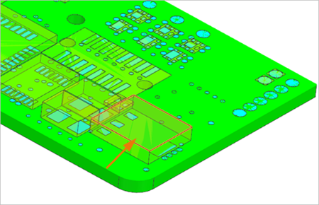
In the graphics window, select the top face of the component as
displayed.
-
In the Pad Region group, click Select
Object
 .
.
- In the Simulation Navigator, expand the PCB_with_pads_fem.fem, hide Polygon Geometry, and show PAD_IC1 (26), PAD_IC1 (27), PAD_IC1 (28), and PAD_IC1 (29) to display the pads' surfaces.
-
In the graphics window, select the 4 pads surfaces under the
component.
- In the Mounting Region group, from the Mounting Region list, select Top Board Region.
-
In the Model Parameters group, set the following values:
- Theta JC = 10 °C/W
- Theta CB = 10 °C/W
- Tmax Case = 105 °C
- Tmax Junction = 110 °C
- Dissipation = 0.5 W
-
In the Underfill Model Parameters group, click
Choose material
 .
.
-
Click Create material
 .
.
- In the Name - Description group, type Thermal Paste.
- In Properties group, in Mass Density (RHO) box, type 2.5E-09 kg/mm3.
-
On the Thermal page, in the
Thermal group, set the following values:
- Thermal Conductivity (K) = 8 W/(m·°C)
- Specific Heat (CP) = 880 J/(kg·K)
- Click OK twice.
- In the PCB Component dialog box, in the Underfill Model Parameters group, in the Thickness box, type 5.5 mm.
- In the Void Fraction box, type 0.4.
- In the Advanced Model Parameters group, in the Junction Capacitance box, type 0 J/°C.
-
In the Description group, set the following
manufacturing characteristics:
- Part Number = DIGIKEY_LT1117CST_5_PBF_ND
- Package = SOT230P700X180-4N
- Manufacturer = Murata
- Click OK.
Create a convection to environment constraint
- In the Simulation Navigator, expand the Simulation Object Container node and hide IC1 to hide the boundary condition in the graphics window.
- Under the PCB_with_pads_fem.fem, show Polygon Geometry to show the PCB component.
-
Choose Home tab→Loads and
Conditions group→Constraint Type
list→Convection to Environment
 .
.
- From the type list, make sure Convection to Environment is selected.
-
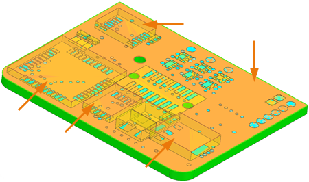
In the graphics window, select the top surface of the 4 displayed
components and the PCB board.
- In the Magnitude - Top group, in the Convection Coefficient box, type 10 W/(m2·°C).
- In the Environment group, from the Temperature list, select Specify.
- In the Temperature Value box, type 20 °C.
- Click OK.
Generate the temperature report
Generate selected thermal solution data for a specified region of your model.
- In the Simulation Navigator, hide Constraint Container.
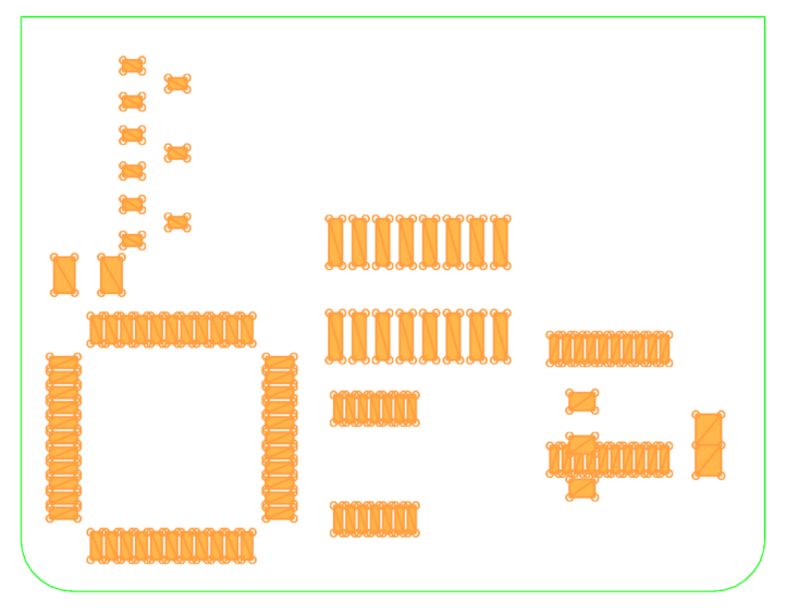
- In the Simulation Navigator, under the PCB_with_pads_fem.fem node, hide Polygon Geometry and show Pads.
-
Choose Home tab→Loads and
Conditions group→Simulation Object
Type list→Report
 .
.
-
In the Region group, select the shown faces.
- In the Thermal Data, select the Temperature check box.
- Click OK.
Solve the model
- In the Simulation Navigator, right-click the Solution 1 node and choose Solve.
- Click OK.
- Wait for the solve to end, before proceeding.
- In the Review Results dialog box, click No.
- In the Analysis Job Monitor dialog box, click Cancel.
- Close the Information window.
Display results
- In the Simulation Navigator, expand the Solution 1 node and double-click the Results node.
- In the Post Processing Navigator, expand the Thermal node and double-click the Temperature - Nodal node.
-
Expand the Post View 1 → Mesh
Collectors → PCB_with_pads_fem.fem →
2D Elements nodes and hide 0D
Elements and 2D Elements except
Pads.
Results show the temperature distribution on pads elements.
Review the HTML report
Explore the HTML file in your analysis directory.
- In the Simulation Navigator, right-click the Solution 1 node and choose Browse.
- Double-click the PCB_with_pads_sim1-Solution_1.GroupReport.htm file to display the report.
-
Observe the temperatures on the selected regions.
You have completed this lab.